Seeing things differently with an electron beam
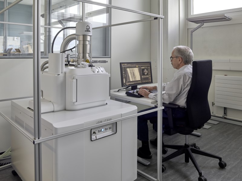
The Geberit Laboratory for Materials Technology recently acquired a scanning electron microscope (SEM) in order to examine surfaces.
Using the SEM, it is now possible to view a small area of a material sample with a magnification of up to 50,000x. In other words, while a resolution in the range of just a few micrometres (micro = one-millionth) can be achieved with conventional optical microscopes, the new SEM has a resolution range of just a few nanometres (nano = one-billionth).
Analysing the composition of materials
The SEM does not work like an optical microscope with visible light; instead, it analyses the sample with the help of an electron beam. You can use a variety of detectors to obtain different information about the sample being analysed, e.g. about its composition. With an optical microscope, the differences in colour and surface structure are visible, but the SEM works in a different way. Using an SEM, you can differentiate between chemical elements, thus allowing you to distinguish between high-alloy and low-alloy steel, for example.
Bringing in existing expertise
SEM analyses were previously outsourced to external service providers, but these did not have much experience of our products and the specific problems we face at Geberit. “Since these analyses can now be carried out internally, the company's internal product expertise can be incorporated into the analysis and interpretation of the results,” comments Thomas Mattle, Head of Technology & Innovation. “Now, all we need are different samples and a little bit of time to be able to develop the sufficient experience.”
More stories


